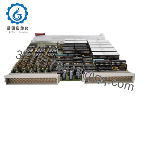
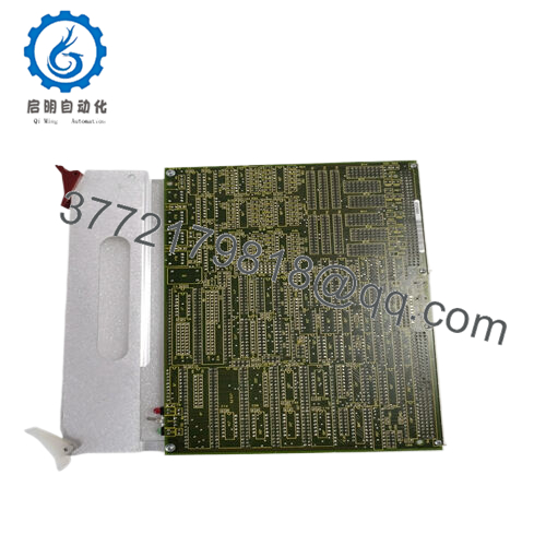
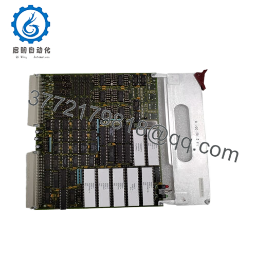
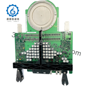
The LAM 810-520659-001 is a specialized printed circuit board (PCB) meticulously engineered by Lam Research, a renowned leader in semiconductor equipment manufacturing. This PCB is not a stand – alone device but an integral part of a larger ecosystem within semiconductor manufacturing equipment.
Model 810-520659-001
Brand Lam Research
Type Printed Circuit Board
The LAM 810-520659-001 is a specialized printed circuit board (PCB) meticulously engineered by Lam Research, a renowned leader in semiconductor equipment manufacturing. This PCB is not a stand – alone device but an integral part of a larger ecosystem within semiconductor manufacturing equipment.
810-520659-001
It is designed to be integrated into the control units of Lam Research’s etching and deposition systems. In the overall architecture of these systems, the LAM 810-520659-001 serves as a communication and control hub. It interfaces with various sensors, actuators, and power sources within the equipment. For example, it receives temperature and pressure data from sensors located within the process chambers and uses this information to adjust the operation of valves and pumps that control gas flow. It also communicates with the power supplies to regulate the energy delivered to the plasma sources or heating elements in the deposition chambers.
For engineers and integrators working in semiconductor manufacturing, the LAM 810-520659-001 is an invaluable component. Its modular design allows for easy integration into existing and new equipment setups. It simplifies the complex task of controlling multiple sub – systems within semiconductor manufacturing equipment, reducing the overall complexity of system design and ensuring smooth and reliable operation.
810-520659-001
Main features and advantages:
One of the primary strengths of the LAM 810-520659-001is its high – speed signal processing capabilities. In semiconductor manufacturing, where processes occur in nanoseconds, the ability to quickly process and respond to signals is crucial. This PCB can rapidly interpret commands from the main control unit and send out precise control signals to the relevant components. For example, when a change in the etching recipe requires an immediate adjustment in the plasma power, the LAM 810-520659-001 can process the new instructions and transmit the appropriate control signals within microseconds, minimizing any disruption to the etching process.
In terms of hardware design, the LAM 810-520659-001 is built to withstand the harsh environment of a semiconductor manufacturing plant. It is constructed with high – quality materials that are resistant to heat, dust, and electrical interference. The PCB’s layout is optimized for efficient heat dissipation, ensuring that it can operate continuously at high temperatures without performance degradation. Its compact size also allows for efficient use of space within the control cabinets of semiconductor equipment, which are often space – constrained.
Compatibility is another major advantage of the LAM 810-520659-001. It is designed to interface seamlessly with a wide range of other components used in semiconductor manufacturing. It can work with different types of sensors, such as mass flow controllers, temperature sensors, and pressure sensors, as well as various actuators like pneumatic valves and electric motors. This versatility simplifies the integration process when upgrading or modifying semiconductor manufacturing equipment, enabling manufacturers to adapt to changing production requirements more easily.
The LAM 810-520659-001 also offers excellent long – term reliability. Lam Research has implemented rigorous quality control measures during its manufacturing process. The PCB is designed to have a long service life, reducing the need for frequent replacements. This not only saves costs but also minimizes the downtime associated with equipment maintenance, ensuring that semiconductor manufacturing plants can operate at maximum productivity.
810-520659-001
Technical specifications:
Model 810-520659-001
Brand Lam Research
Type Printed Circuit Board
Contact Us Phone:+86 16626708626 WeChat/WhatsApp:+86 16626708626 Email: 3772179818@qq.com
Application areas:
In the highly intricate and demanding domain of semiconductor manufacturing, precision and reliability are non – negotiable. The LAM 810-520659-001 plays a pivotal role within this industry, specifically in the operation of advanced etching and deposition equipment.
Semiconductor fabrication plants rely on etching processes to remove unwanted material from silicon wafers with extreme accuracy. The LAM 810-520659-001 is often integrated into the control systems of etching tools. For instance, in the creation of complex integrated circuits, it helps manage the power distribution and signal control for the plasma sources used in dry etching. Precise control of the plasma’s characteristics, such as its density and energy, is crucial. If the power to the plasma source fluctuates due to a malfunctioning control component, it can lead to uneven etching. This, in turn, may result in defective semiconductor chips, which are costly to discard and can disrupt the entire production line.
In deposition processes, which involve layering thin films of materials onto wafers, the LAM 810-520659-001 also has a significant contribution. It can be responsible for regulating the gas flow rates and pressures within the deposition chambers. Different semiconductor devices require specific thicknesses and compositions of these deposited layers. The LAM 810-520659-001 ensures that the deposition process adheres to these exacting standards. In the production of high – performance memory chips, for example, the proper deposition of materials like silicon dioxide and polysilicon is essential for the chip’s functionality. Any deviation in the deposition process, which could be caused by incorrect gas flow control, can lead to memory read – write errors.
Related products:
LAM 810 – 017086 – 006 – Another PCB in Lam Research’s product line, often used in similar semiconductor manufacturing equipment control applications. It may have some overlapping functionality with the LAM 810 – 520659 – 001 but could be optimized for different sub – processes or have different signal – handling capabilities.
LAM 810 – 017034 – 003 – A CPU – related board that can interface with the LAM 810 – 520659 – 001 in more complex control setups within semiconductor manufacturing equipment. Together, they can manage the overall operation of the equipment, with the LAM 810 – 017034 – 003 handling some of the computational tasks and the LAM 810 – 520659 – 001 managing the signal distribution and control.
LAM 810 – 550099 – 001 – A PCB that may be used in parallel or in a complementary manner with the LAM 810 – 520659 – 001 for specific functions within semiconductor manufacturing. It could be involved in tasks such as power management or additional signal processing, enhancing the overall performance of the control system.
LAM 810 – 017086 – 008 – This board is also designed for semiconductor manufacturing control. It can work in tandem with the LAM 810 – 520659 – 001 in systems where multiple PCBs are required to handle different aspects of the manufacturing process, such as separate control of etching and deposition steps in a combined equipment setup.
LAM 810 – 057050 – 003 – A board that might have some compatibility with the LAM 810 – 520659 – 001 in terms of communication protocols and system integration. It could be used in a modular control system where different boards, including the LAM 810 – 520659 – 001 and LAM 810 – 057050 – 003, work together to achieve the overall control of semiconductor manufacturing processes.
Installation and maintenance:
Before installing the LAM 810 – 520659 – 001, it is crucial to carefully plan the layout within the control cabinet. Ensure that there is sufficient clearance around the PCB to allow for proper ventilation. Semiconductor manufacturing environments can be hot, and effective heat dissipation is essential for the PCB’s performance and longevity. The control cabinet should also be properly grounded to prevent electrical interference that could disrupt the PCB’s operation. Check the mounting points and ensure they are clean and free from any debris or corrosion to ensure a secure and stable installation.
For maintenance, regular visual inspections are highly recommended. Look for any signs of physical damage, such as cracks in the PCB, loose components, or signs of overheating like discoloration. Periodic electrical testing should also be carried out to verify the integrity of the signals passing through the PCB. This can involve using specialized testing equipment to measure voltage levels, signal frequencies, and impedance. Keep the PCB clean by using appropriate cleaning methods to remove dust and other contaminants that could potentially affect its performance. Additionally, stay updated with any firmware or software updates provided by Lam Research, as these can often improve the PCB’s functionality, fix bugs, and enhance its compatibility with other components in the semiconductor manufacturing system.

 WhatsApp: +86 16626708626
 Email: 3772179818@qq.com
 Phone: +86 16626708626