LAM 810-234640-312 high – performance printed circuit board
LAM 810-234640-312 high – performance printed circuit board
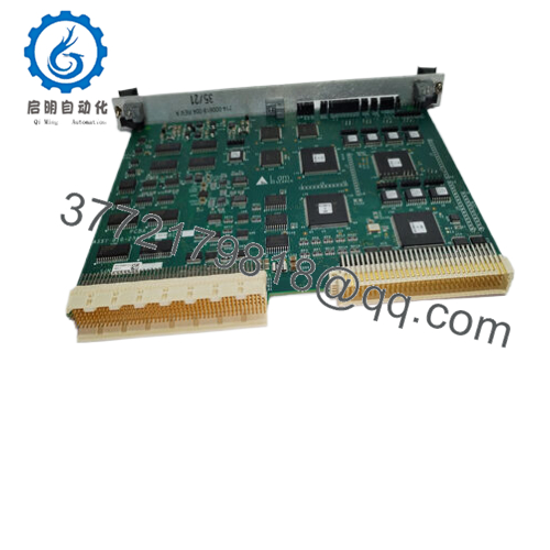
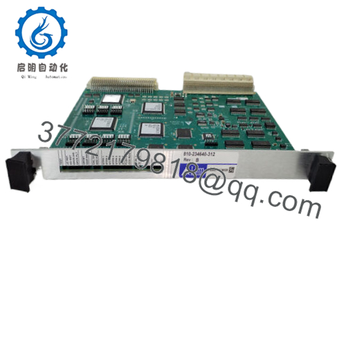
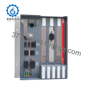
The LAM 810-234640-312 is a high – performance printed circuit board meticulously designed and manufactured by Lam Research, a globally recognized leader in semiconductor equipment. As a key component within semiconductor manufacturing equipment, it serves as a nerve center, facilitating the communication and control of multiple sub – systems.
Model LAM 810-234640-312
Brand LAM Research
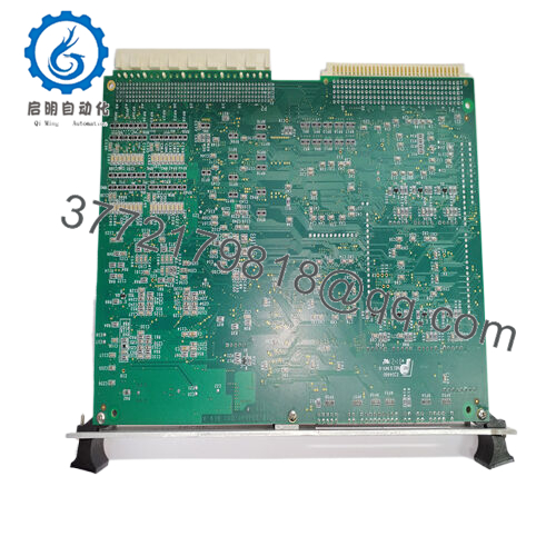
Type Printed Circuit Board Assembly
Mounting screw – mounted, snap – in
Interfaces RS – 232, etc.
Cooling Natural convection, forced – air cooling, etc.
The LAM 810-234640-312 is a high – performance printed circuit board meticulously designed and manufactured by Lam Research, a globally recognized leader in semiconductor equipment. As a key component within semiconductor manufacturing equipment, it serves as a nerve center, facilitating the communication and control of multiple sub – systems.
810-234640-312
This PCB is part of Lam Research’s advanced product portfolio for semiconductor manufacturing systems. It is engineered to be integrated into the larger control architecture of etching and deposition equipment. In the overall system, it acts as an intermediary between the main control unit and the various actuators, sensors, and power sources. It receives high – level commands from the control unit, decodes them, and then sends out precise electrical signals to the relevant components to execute the desired manufacturing process steps.
For engineers and integrators working in semiconductor manufacturing, the LAM 810-234640-312 is invaluable. Its modular design allows for easy customization and integration into existing and new equipment setups. It provides a reliable and efficient solution for managing the complex electrical requirements of semiconductor manufacturing processes, reducing the overall complexity of system design and ensuring smooth operation of the manufacturing line.
810-234640-312
Main features and advantages:
One of the standout features of the LAM 810-234640-312 is its exceptional signal integrity. In the high – speed and high – precision environment of semiconductor manufacturing, maintaining accurate and noise – free electrical signals is crucial. This PCB is designed with advanced trace routing and shielding techniques to minimize electromagnetic interference, ensuring that the signals sent to and from various components are transmitted without distortion. This high – level signal integrity directly contributes to the precision and repeatability of the etching and deposition processes.
In terms of hardware design, the LAM 810-234640-312 is built to withstand the harsh conditions within a semiconductor manufacturing plant. It has a rugged construction that can endure high temperatures, humidity, and vibrations. The use of high – quality materials in its fabrication ensures long – term reliability, reducing the need for frequent replacements and minimizing downtime. Additionally, its compact size allows for efficient use of space within the control cabinets of semiconductor equipment, which are often space – constrained.
Compatibility is another major strength of this PCB. It is engineered to interface seamlessly with a wide range of other components used in semiconductor manufacturing. It can work with different types of sensors, such as temperature sensors, pressure sensors, and gas flow sensors, as well as various actuators like valves and motors. This versatility simplifies the integration process when upgrading or modifying semiconductor manufacturing equipment, enabling manufacturers to adapt to changing production requirements more easily.
The LAM 810-234640-312 also offers excellent thermal management capabilities. With the high – power components used in semiconductor manufacturing, heat generation is a significant concern. This PCB is designed with an optimized layout and heat – dissipating features, such as thermal vias and copper planes, to efficiently transfer heat away from sensitive components. This helps to maintain the operating temperature within the optimal range, further enhancing the long – term reliability and performance of the PCB.
810-234640-312
Technical specifications:
Model LAM 810-234640-312
Brand LAM Research
Type Printed Circuit Board Assembly
Mounting screw – mounted, snap – in
Interfaces RS – 232, etc.
Cooling Natural convection, forced – air cooling, etc.
Contact Us Phone:+86 16626708626 WeChat/WhatsApp:+86 16626708626 Email: 3772179818@qq.com
810-234640-312
Application areas:
In the highly competitive and technologically advanced realm of semiconductor manufacturing, every component plays a pivotal role in ensuring the seamless operation of complex processes. The LAM 810-234640-312 printed circuit board (PCB) is no exception. This specialized PCB is predominantly utilized within the intricate control systems of semiconductor etching and deposition equipment, which are the workhorses of semiconductor fabrication plants.
Semiconductor etching is a precision – based process where unwanted material is removed from silicon wafers with extreme accuracy. The LAM 810-234640-312 PCB is designed to manage and regulate the electrical signals that control the various components involved in this process. For example, it interfaces with the power supplies that drive the high – energy plasma used in etching. Precise control of the plasma’s power and characteristics is crucial, as any deviation can lead to uneven etching, resulting in defective semiconductor chips. In a state – of – the – art semiconductor manufacturing facility, where thousands of chips are produced per day, such defects can translate into significant financial losses.
Deposition processes, on the other hand, involve adding thin layers of materials onto the wafers. The LAM 810-234640-312 also plays a role here, coordinating the operation of gas delivery systems, temperature sensors, and deposition chambers. It ensures that the right amount of material is deposited at the correct temperature and pressure, maintaining the integrity and quality of the deposited layers. This is essential for the production of advanced semiconductor devices such as high – performance microprocessors, memory chips, and sensors, which are the building blocks of modern electronics, from smartphones to supercomputers.
810-234640-312
Related products:
LAM 810 – 069751 – 102 – Another PCB in Lam Research’s product line, often used in similar semiconductor manufacturing equipment control applications, but may have different pin – out configurations or signal – handling capabilities for specific sub – processes.
LAM X10 – 14210100 – It belongs to the same family of VIOP (Voltage, Current, and Power) related PCBs. It can be used in parallel or in a complementary manner with the LAM 810 – 234640 – 312 for more complex control scenarios within semiconductor equipment.
LAM 810 – 234640 – 311 – A closely related PCB model. While sharing many similarities with the LAM 810 – 234640 – 312, it may have minor differences in terms of component layout or functionality, perhaps optimized for a slightly different set of semiconductor manufacturing processes.
LAM 810 – 046015 – 009 – This PCB is also designed for semiconductor manufacturing control. It can interface with the LAM 810 – 234640 – 312 in systems where multiple PCBs are required to handle different aspects of the manufacturing process, such as separate control of etching and deposition steps in a combined equipment setup.
LAM 810 – 099175 – 011 – It is used in semiconductor equipment control systems and can work in tandem with the LAM 810 – 234640 – 312 to provide additional functionality, like redundant control paths or enhanced signal processing for more critical manufacturing operations.
Installation and maintenance:
Before installing the LAM 810-234640-312, it is essential to carefully plan the layout within the control cabinet. Ensure that there is sufficient clearance around the PCB to allow for proper ventilation. Since semiconductor manufacturing environments can be hot, effective heat dissipation is crucial for the PCB’s performance and longevity. The control cabinet should also be properly grounded to prevent electrical interference that could disrupt the PCB’s operation. Check the mounting points and ensure they are clean and free from any debris or corrosion to ensure a secure and stable installation.
For maintenance, regular visual inspections are recommended. Look for any signs of physical damage, such as cracks in the PCB, loose components, or signs of overheating like discoloration. Periodic electrical testing should also be carried out to verify the integrity of the signals passing through the PCB. This can involve using specialized testing equipment to measure voltage levels, signal frequencies, and impedance. Keep the PCB clean by using appropriate cleaning methods to remove dust and other contaminants that could potentially affect its performance. Additionally, stay updated with any firmware or software updates provided by Lam Research, as these can often improve the PCB’s functionality, fix bugs, and enhance its compatibility with other components in the semiconductor manufacturing system.

 WhatsApp: +86 16626708626
 Email: 3772179818@qq.com
 Phone: +86 16626708626