 WhatsApp: +86 16626708626
 Email:
  Phone: +86 16626708626
Description
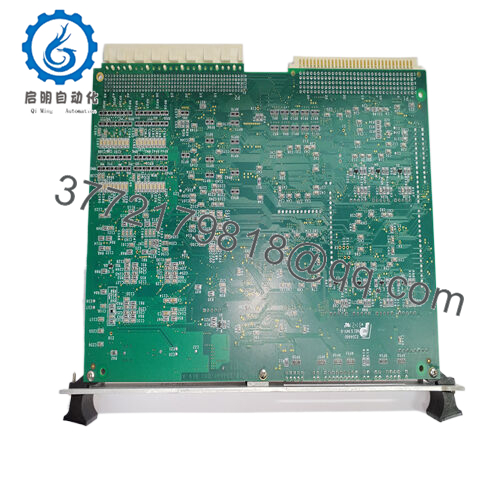
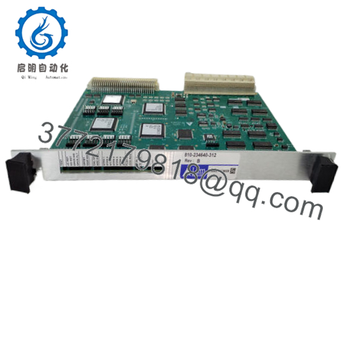
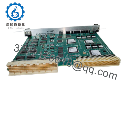
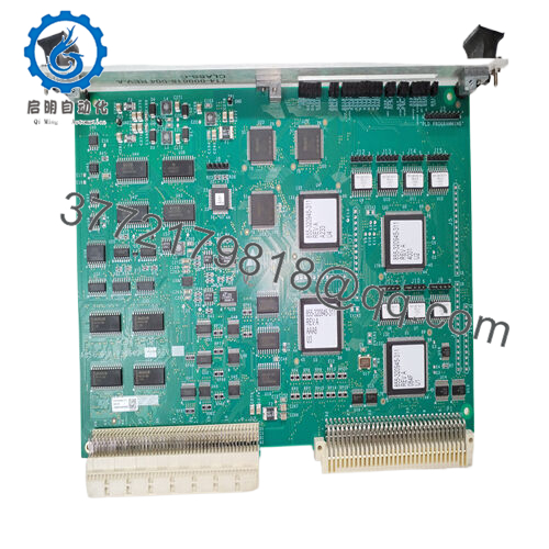
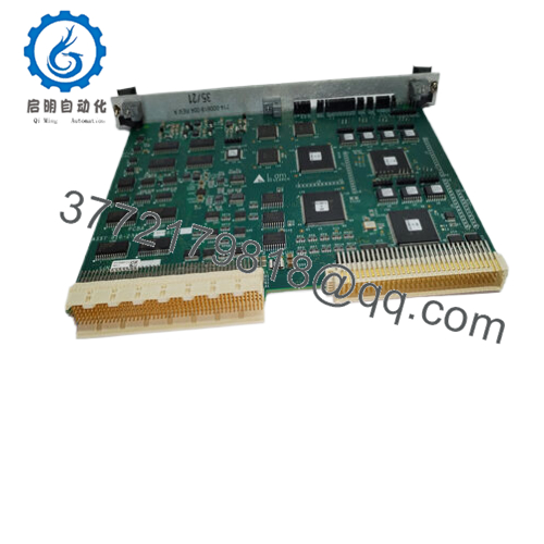
The LAM 810-234640-312 is a highly specialized VIOP (Voltage Input/Output Processor) Phase III Printed Circuit Board (PCB) Board used primarily in advanced semiconductor manufacturing equipment. This board plays a vital role in managing critical electrical signals related to voltage input and output, supporting precise control and monitoring functions essential in semiconductor fabrication processes. The module is engineered to maintain signal integrity and support high-speed data acquisition and transmission, crucial for delicate process control in fabs.
Widely integrated into Lam Research tools and similar high-tech semiconductor manufacturing systems, the LAM 810-234640-312 works by enhancing communication between various control subsystems and the main process controllers. It ensures accurate voltage regulation and monitoring necessary for sustaining process consistency, defect reduction, and yield optimization during manufacturing of complex devices like 3D NAND structures.
Functionally, the LAM 810-234640-312 PCB board serves as the voltage interface processor within automated manufacturing equipment, delivering reliable voltage signal conditioning, error correction, and amplification. It is designed to work seamlessly within multi-layer PCB architectures supporting complex signal routing and noise isolation. This makes it indispensable for controlling power distribution and monitoring on critical manufacturing processes.
The board adheres to strict industry standards for dimensions and electrical performance, facilitating straightforward replacement or system upgrades. Its robust construction and sophisticated internal layout ensure performance stability under typical semiconductor fab environmental conditions, including temperature and humidity control requirements.

- 810-234640-312
The LAM 810-234640-312 boasts multiple advantages including high channel density, improved signal-to-noise ratios, and enhanced thermal management. Its multi-layer PCB design enables signal shielding and isolation to minimize electromagnetic interference—a common challenge in semiconductor fabs. The PCB supports resistant materials and advanced soldering techniques ensuring longevity and durability even under prolonged heavy usage.
A compact and modular design allows easy integration into larger PCB assemblies, with precise manufacturing tolerances that promote consistent quality across production runs. The LAM 810-234640-312 is verified for compatibility with industry-standard system interfaces, making it flexible for use in existing as well as next-generation fab equipment.
| Parameter | Value |
|---|---|
| Model | LAM 810-234640-312 |
| Brand | LAM Research |
| Type | VIOP Phase III PCB Board |
| Application | Semiconductor manufacturing equipment |
| Function | Voltage Input/Output processing |
| Construction | Multi-layer PCB, high-density signal routing |
| Operating Conditions | Semiconductor fab environment |
| Weight | Approx. 1.26 kg |
| Dimensions | Standard Lam Research board dimensions |
| Compatibility | Industry standard control systems |
Modules related or compatible with the LAM 810-234640-312 include:
LAM 810-234640-311 – A similar VIOP PCB board with variations in electrical configurations.
LAM 810-099175-011 – Phase III PCB board for voltage control in semiconductor equipment.
LAM 810-068158-014 – Node robot interface PCB commonly used alongside voltage control boards.
LAM 810-800081-022 – Controller module complementing VIOP boards in process control systems.
LAM 853-049542-173 – Temperature control multi-channel PCB supporting overall process stability.
Installation of the LAM 810-234640-312 requires adherence to strict cleanroom and electrostatic discharge (ESD) handling procedures to protect sensitive circuitry. The PCB should be installed in designated slots with secure mounting to minimize mechanical stress and vibration impacts. Power and signal cables must be routed carefully with appropriate shielding to maintain signal integrity.
Routine inspection and cleaning of the PCB assembly, along with verification of electrical connections, support optimal operation. Firmware and system software supporting these boards should be kept updated to ensure compatibility and performance enhancements over time.