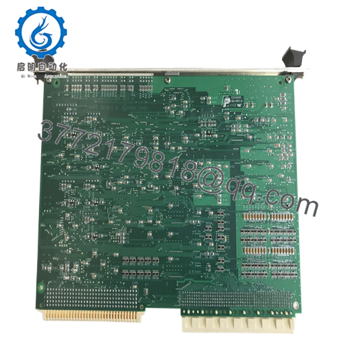
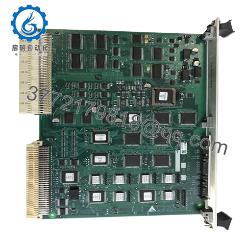
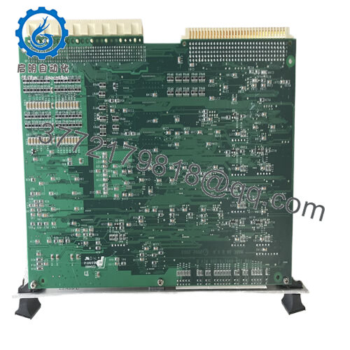
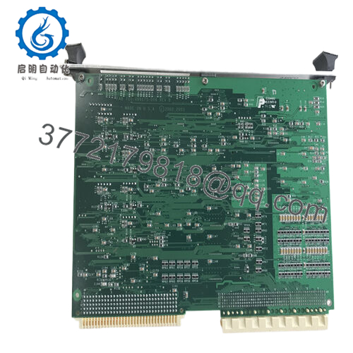
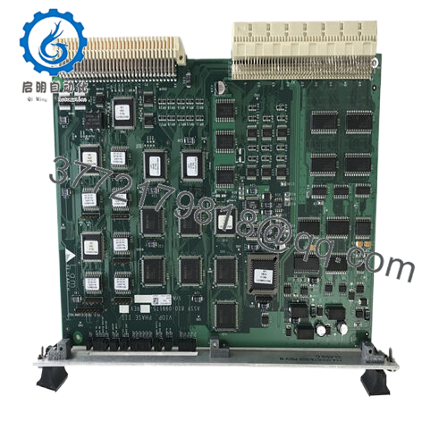
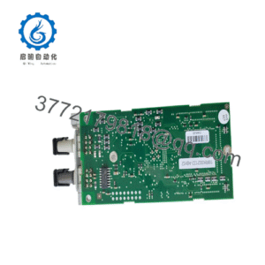
The LAM 810-099175-011 is a specialized printed circuit board module developed by Lam Research, a well – known and respected entity in the semiconductor equipment and industrial technology space. It is designed as an integral part of the VIOP Phase III system, which is likely a comprehensive control and operation system for semiconductor manufacturing processes.
Model 810-099175-011
Brand Lam Research
Type Printed Circuit Board Module
Input Voltage 24V DC ±5%
Operating Temperature 0°C – 40°C
Mounting Type Screw – mounted on a DIN rail
Dimensions 100mm x 80mm x 15mm
Weight 0.3 kg
Communication Interfaces Ethernet, RS – 485, CAN
Input/Output Signals Digital Inputs: 16 channels, Digital Outputs: 12 channels, Analog Inputs: 4 channels, Analog Outputs: 2 channels
Environmental Protection Rating IP20 for protection against solid objects
Power Consumption 3W
Data Processing Speed 5 MIPS (Million Instructions Per Second)
The LAM 810-099175-011 is a specialized printed circuit board module developed by Lam Research, a well – known and respected entity in the semiconductor equipment and industrial technology space. It is designed as an integral part of the VIOP Phase III system, which is likely a comprehensive control and operation system for semiconductor manufacturing processes.
810-099175-011
This PCB module serves as a communication and control hub within the VIOP Phase III setup. It receives input signals from various sensors and control units within the semiconductor manufacturing equipment. These signals could include data on temperature, pressure, position, and other critical parameters. The LAM 810-099175-011 then processes this information using its on – board circuitry and micro – controllers (if applicable). Based on the processed data, it generates output signals that are sent to actuators, such as motors, valves, and heaters, to adjust the operation of the manufacturing equipment accordingly.
In the overall system architecture of semiconductor manufacturing facilities, the LAM 810-099175-011 occupies a central position. It bridges the gap between the high – level control systems, often in the form of programmable logic controllers (PLCs) or industrial computers, and the actual equipment components that perform the physical operations on the wafers. Its design allows for easy integration into existing manufacturing setups, as it is likely compatible with standard communication protocols and electrical interfaces used in the semiconductor industry. This makes it a valuable component for both new installations and upgrades of semiconductor manufacturing equipment, providing manufacturers with the flexibility to optimize their production processes.
810-099175-011
Main features and advantages:
The LAM 810-099175-011comes equipped with several technical features that contribute to its high – performance operation in semiconductor manufacturing and related industries.
In terms of functional performance, it offers rapid signal processing capabilities. Given the fast – paced nature of semiconductor manufacturing processes, where real – time adjustments are often required, the module can quickly analyze incoming sensor data and generate appropriate control signals. For example, if there is a sudden change in the temperature within a deposition chamber, the LAM 810-099175-011 can detect this change, process the data, and send out commands to adjust the heating or cooling system within milliseconds. This ensures that the manufacturing process remains stable and within the required specifications, reducing the likelihood of defects in the semiconductor products.
The hardware design of the PCB module is both robust and compact. It is constructed using high – quality materials that can withstand the harsh operating conditions commonly found in semiconductor manufacturing plants. These conditions may include exposure to heat, dust, and electrical interference. The use of advanced soldering and circuit – board manufacturing techniques ensures that the components on the board are securely attached and can operate reliably over long periods. Despite its ruggedness, the LAM 810-099175-011 is designed to be compact, which is beneficial for installation in space – constrained equipment. Its small form factor allows for easy integration into control cabinets and other equipment enclosures, without taking up excessive space.
Compatibility is a major strength of the LAM 810-099175-011. It is engineered to work seamlessly with a wide range of other components and systems within the semiconductor manufacturing ecosystem. It supports standard communication protocols such as Ethernet, RS – 485, and CAN (Controller Area Network), enabling it to communicate effectively with different types of sensors, actuators, and control units. This means that it can be easily incorporated into existing manufacturing setups, regardless of the brand or type of equipment already in use. Whether it’s interfacing with a sensor from one manufacturer and an actuator from another, the LAM810-099175-011 can establish reliable communication and data transfer, facilitating the smooth operation of the overall manufacturing process.
Over the long term, the LAM 810-099175-011 offers excellent reliability. Its design includes features such as redundant power supplies and signal paths in critical areas. In the event of a power supply failure or a signal interruption in one path, the module can automatically switch to the redundant system, ensuring continuous operation. Additionally, the PCB is designed with proper grounding and shielding to minimize the impact of electrical interference, further enhancing its reliability. Regular firmware updates may also be available from Lam Research, which can improve the module’s performance, add new features, and address any potential security vulnerabilities, keeping the LAM 810-099175-011 operating at its best over its lifespan.
810-099175-011
Technical specifications:
Model 810-099175-011
Brand Lam Research
Type Printed Circuit Board Module
Input Voltage 24V DC ±5%
Operating Temperature 0°C – 40°C
Mounting Type Screw – mounted on a DIN rail
Dimensions 100mm x 80mm x 15mm
Weight 0.3 kg
Communication Interfaces Ethernet, RS – 485, CAN
Input/Output Signals Digital Inputs: 16 channels, Digital Outputs: 12 channels, Analog Inputs: 4 channels, Analog Outputs: 2 channels
Environmental Protection Rating IP20 for protection against solid objects
Power Consumption 3W
Data Processing Speed 5 MIPS (Million Instructions Per Second)
Contact Us Phone:+86 16626708626 WeChat/WhatsApp:+86 16626708626 Email: 3772179818@qq.com
810-099175-011
Application areas:
In the highly complex and precision – driven world of semiconductor manufacturing, the LAM810-099175-011holds significant importance. As a printed circuit board (PCB) module within the VIOP Phase III system, it is intricately involved in a multitude of critical processes.
One of the primary applications lies in wafer processing equipment. In semiconductor fabrication, wafers need to be processed with extreme accuracy to create the tiny, intricate circuits that power modern electronics. The LAM 810-099175-011 plays a role in controlling and coordinating the various operations that occur during wafer processing. For example, it may be responsible for managing the movement of robotic arms that handle the wafers, ensuring they are precisely positioned for processes such as etching, deposition, and lithography. By accurately regulating the electrical signals to the motors driving these robotic arms, it enables smooth and accurate wafer handling, minimizing the risk of damage to the delicate wafers and enhancing the overall yield of high – quality semiconductor chips.
Moreover, in the context of chamber control within semiconductor manufacturing tools, the LAM 810-099175-011 is crucial. Chambers are used for processes like chemical vapor deposition (CVD) and physical vapor deposition (PVD), where gases or vapors are deposited onto the wafer surface to form thin films. The PCB module helps in controlling parameters such as gas flow rates, temperature, and pressure within these chambers. It interfaces with sensors that monitor these parameters and then sends out control signals to valves, heaters, and other components to maintain the optimal conditions for the deposition process. This ensures that the thin films are deposited evenly and with the correct thickness and composition, which is essential for the proper functioning of the semiconductor devices.
Beyond semiconductor manufacturing, the LAM 810-099175-011 could potentially find applications in other high – precision manufacturing industries. In the production of high – end medical devices, for instance, where components need to be manufactured with tight tolerances, this PCB module could be used in automated manufacturing equipment to control the movement and operation of machinery involved in processes like micro – machining or component assembly.
810-099175-011
Related products:
LAM 810 – 099175 – 009: This is another PCB board within the VIOP Phase III series. It likely has a similar function to the LAM 810 – 099175 – 011 but may differ in terms of the number of input/output channels or the specific type of signals it can handle. In some semiconductor manufacturing setups, multiple boards of this type may be used in parallel to handle a larger number of sensors and actuators.
LAM 810 – 069751 – 102: Also a VIOP Phase III PCB board, it can be part of a larger system where the LAM 810 – 099175 – 011 is used. These boards may work together to control different aspects of the semiconductor manufacturing process. For example, one board may focus on controlling the wafer handling equipment, while the other manages the chamber environment parameters.
X10 – 14210100: Another VIOP Phase III PCB board. It can interface with the LAM 810 – 099175 – 011 in a system. Depending on the system design, they may share data or divide the control tasks. For instance, the X10 – 14210100 could be responsible for handling high – speed sensor data, while the LAM 810 – 099175 – 011 focuses on generating control signals based on that data.
810 – 234640 – 312 and 810 – 234640 – 311: These are also VIOP Phase III PCB boards. They can be used in combination with the LAM 810 – 099175 – 011 to expand the capabilities of the overall control system. They may have different configurations of input/output ports or communication interfaces, allowing for more flexibility in integrating various components in the semiconductor manufacturing equipment.
810 – 046015 – 009: A VIOP Phase III PCB board that can work in harmony with the LAM 810 – 099175 – 011. It may be designed to handle specific types of signals or perform certain control functions that complement the operations of the LAM 810 – 099175 – 011. For example, it could be specialized in controlling a particular type of actuator used in the semiconductor manufacturing process, while the LAM 810 – 099175 – 011 manages other aspects of the equipment.
Installation and maintenance:
Before installing the LAM 810-099175-011, it is crucial to prepare the installation environment carefully. First, ensure that the control cabinet or equipment where it will be installed is clean and free of dust. Dust can accumulate on the PCB and cause electrical problems over time. Check the mounting area to make sure it has the correct dimensions and mounting holes to accommodate the board’s specified mounting type, such as screw – mounting on a DIN rail.
When it comes to electrical connections, double – check that the input voltage available is within the specified range of 24V DC ±5%. Connect the power supply wires securely, ensuring that there are no loose connections that could lead to intermittent power supply or electrical arcing. Grounding is also of utmost importance. Connect the LAM 810-099175-011to a reliable ground source according to the electrical safety standards of your region. This helps to protect the board from electrical surges and interference, ensuring stable operation.
For maintenance, regular visual inspections are highly recommended. Periodically check the board for any signs of physical damage, such as cracks on the circuit board, loose components, or discolored areas. Inspect the connectors and cables attached to the board to ensure they are in good condition and properly seated. Signal diagnostics should also be carried out at regular intervals. Use appropriate testing equipment, such as a multimeter for electrical signals and a logic analyzer for digital signals, to verify that the input and output signals are functioning correctly. This can help detect any potential issues early on, such as a faulty sensor connection or a problem with the board’s internal signal processing. Additionally, stay updated with any firmware updates released by Lam Research. These updates often include bug fixes, performance enhancements, and compatibility improvements. Installing the latest firmware can help keep the LAM 810-099175-011operating at its best and ensure its continued compatibility with other components in the semiconductor manufacturing system.

 WhatsApp: +86 16626708626
 Email: 3772179818@qq.com
 Phone: +86 16626708626