
 WhatsApp: +86 16626708626
 Email:
  Phone: +86 16626708626
Description
What This Product Solves
In the unforgiving precision of semiconductor etching and process control environments, detecting and aligning wafer edges with sub-millimeter accuracy is non-negotiable—particularly in Lam Research platforms like the TCP 9600 or Kiyo etchers, where even a 0.5mm misalignment during load can offset plasma exposure, etching features asymmetrically and introducing CD variations that cascade into electrical failures, yield drops exceeding 3%, and forced requalifications that idle tools for days in fabs under the hammer of SEMI E10 uptime mandates and node-shrinking timelines to 2nm. These alignment pitfalls sharpen during high-volume lots or chamber quals, where dust from wafer handling or thermal distortions in sensors corrupt edge signals, compelling conservative centering that throttles throughput or risks overexposure defects, amplifying the engineering strain in cleanrooms where every micron matters to margin and market speed.
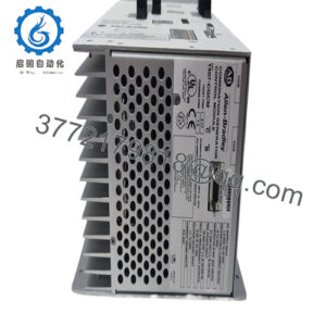
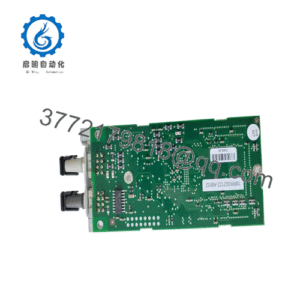
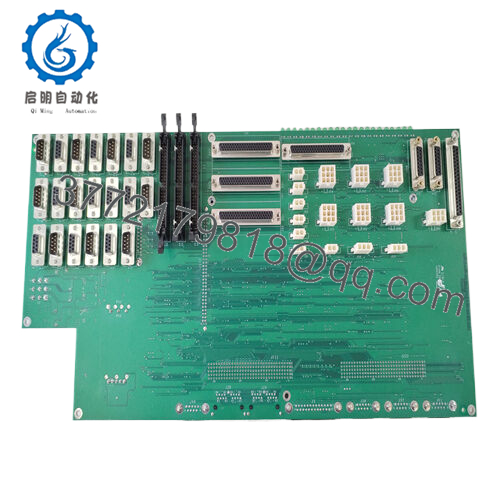
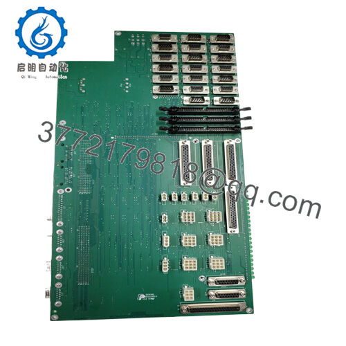
The Lam Research 810-082745-003 meets this as a PCB Edge Detector Junction Board, a specialized interface engineered to aggregate and condition signals from optical or capacitive edge sensors in Lam’s etch tools, delivering robust detection that ensures centered wafer placement without the false triggers that fragment focus rings or scar substrates. It’s a key enabler in retrofits for 300mm clusters or expansions into multi-wafer processing, where modular integration requires junction boards that splice sensor arrays into the VIOP controller without signal degradation. For engineers navigating high-reliability challenges in industrial automation for wafer handling, this PCB intervenes when generic multiplexers succumb to EMI from RF match networks or vibration from robot arms, providing the junction isolation that upholds I/O signal integrity across dusty, high-vibe bays.
Imagine a gate etch where the board must fuse dual-sensor data to offset bow-induced tilts before igniting 1kW plasmas, or a contact via step where edge interrupts halt on <0.2mm deviations to avert fencepost errors—the Lam Research 810-082745-003 excels, with its buffered channels and threshold logic that filters noise while propagating clean interrupts. In these semiconductor process control forges, it reduces the debug drag of alignment audits, enabling HMI overlays that spotlight sensor skews early. Fundamentally, this edge detector board recasts wafer centering from a calibration curse to a confidence constant—fostering the placement precision and process purity that safeguards yields, while easing the path to scalable handling in your fab’s high-volume horizon where every edge etches excellence.
How the Product Works & Fits into a System
The Lam Research 810-082745-003 operates as a signal aggregator in Lam etch architectures, channeling up to 8 differential inputs from edge sensors via opto-isolated buffers that condition 0-5V pulses for <1ms rise times, then multiplexing them through a junction ASIC to output TTL-compatible interrupts over RS422 to the VIOP controller—employing configurable thresholds to debounce artifacts from substrate warpage or particle shadows, all while sourcing 5V/24V from the backplane to tolerate 500V transients from electrostatic chucks. It self-calibrates on init via onboard pots for zero-offset, flags marginal signals with a status LED, and integrates fault relays that e-stop on total occlusion, ensuring SEMI E57-compliant wafer mapping without latency lags.
Nestled in the alignment and I/O stratum of your tool’s stack, it junctions into a sensor breakout panel via ribbon cables, interfacing upstream with the MACH front-end over twisted pairs for 50m runs and downstream to fiber-optic or laser detectors through BNC or mini-DIN—suited for redundant detection where dual boards cross-validate edges, failing to a safe retract on discrepancy to prevent misloads. Protocol handling includes Lam’s proprietary EDJ dialect with GEM E30 echoes for fab traceability, adjustable via console tweaks to tune for process-specific substrates like SOI wafers.
Diagnostics are straightforward: per-channel status indicators and a test loop for bench simulation that mimics edge passes, piping traces to the HMI for profile plotting—no signal generator required. In a comprehensive configuration, it flanks the robot controller upstream and chuck actuators downstream, forming a vigilant vanguard for verified placements—like in a Flex breakthrough etch where it confirms edge centering before bias ramp, interlocking with vacuum sensors for planar assurance. For a TCP 9400 retrofit, the Lam Research 810-082745-003 would consolidate legacy detectors, compensating for fiber bends to sustain <0.1mm resolution. This seamless splicing streamlines sensor swaps, positioning it as the perceptive pivot in your placement pipeline, fusing field flashes with frame fidelity for attuned, aberration-free advancement.

- 810-073479-215
| Specification | Details |
|---|---|
| Model Number | 810-082745-003 |
| Brand | Lam Research |
| Type | PCB Edge Detector Junction Board |
| Input Voltage | 5 VDC / 24 VDC (backplane) |
| Operating Temp Range | 0°C to 50°C |
| Mounting Style | Junction Panel / Ribbon Cable |
| Dimensions | 7 x 5 x 0.6 in |
| Weight | 0.4 lb |
| Interface/Bus | RS422 Serial / Sensor I/O |
| Compliance | SEMI E57, CE, RoHS |
| Supported Protocols | Lam EDJ, GEM E30 |
| Typical Power Draw | 4 W |
Real-World Benefits
Opting for the Lam Research 810-082745-003 fortifies your Lam etchers with a junction board honed for the hyper-precise handoffs of high-volume handling, where its isolated buffering and threshold agility confine detection jitter to <0.05ms—translating to wafer offsets below 0.1mm across bowed 300mm plates, empowering uniform etches that trim CD sigma by 0.3nm without the frequent recalibrations that sensor sprawls necessitate. This acuity isn’t anomalous; it aligns across runs, enabling dynamic mapping where edge data adapts to film stacks for defect maps dipping under 0.02/cm², distilling qual quarantines into quick quals over lot-long labors.
Alignment crews appreciate its alert architecture, as channel vetoes and interrupt audits surface sensor fouling in the GEM grid—envision a shift tech tracing a dust-darkened fiber from trend ticks, cleaning cycle-free sans centering chaos. The board’s panel pliancy lightens integration loads, cable-compatible with Kiyo subracks that forgo fixture fiddles, hastening handler handovers in throughput-thrashed fabs where wafer waits weigh woes. Over fab epochs of 6+ years, it upholds detection durability with a MTBF over 120,000 hours, its shielded traces thwarting photoresist particulates in loadlocks, so your edge ensembles evolve without the erosion of erratic excursions.
Deeper, the Lam Research 810-082745-003 encourages extensibility by exposing aux triggers for metrology, layering in AI where detection pulses pair with scatterometry for predictive placements—priming for 450mm migrations sans sensor surgeries. These intertwined insights recast edge detection from a handling hassle to a handling hallmark, curbing total tool tallies while amplifying the alignment that advances your semiconductor supremacy.
Typical Use Cases
The Lam Research 810-082745-003 anchors in transformer coupled plasma etchers like the TCP 9600, paneling into junction bays to poll capacitive edges for pre-etch centering, where its <0.1mm res holds amid 13.56MHz fields and SF6 flows—core to process control environments trenching trenches under 7nm, shoring critical system uptime through cassette cascades or qual quenches in memory module fabs. In these sulfurous sanctums, its debounce fortifies signal reliability, provisioning placement purity that parries undercuts and uniformity ullages.
Photoresist strip bays beckon it for post-litho alignment, aggregating optical interrupts from lift pins and stage fiducials under 500W O2 plasmas and N2 sweeps, fostering continuous uptime where fast data cycles from cameras decree residue removal radii. Harsh ash accumulations and thermal tilts test its tenacity, yet it yields unyielding unity for flawless field flats.
In dual-beam focus etch clusters, the Lam Research 810-082745-003 marshals Kiyo spacer etches, fusing laser lineouts with discrete detectors over sensor splices—pivotal for used in finFET formation where edge exactitude evades encapsulation errors and fin fanouts. Across TCP etching, ash stripping, and spacer sculpting sectors, this junction board jumpstarts applications demanding detection dominion in discharge domains, transmuting edge echoes into edifices of etch excellence.
810-082745-004 – Rev D variant with expanded channels for multi-sensor 450mm handling.
810-099175-011 – VIOP Phase III companion for motion-synced edge detection.
685-247270-001 – FE-HD1 MACH add-on for front-end sensor aggregation.
810-234640-312 – Chamber mux for etch-specific edge discrete extensions.
810-800081-022 – P2MB bridge for mainframe-to-junction interfacing.
810-102361-222 – Analog detector PCB for telemetry-blended edges.
810-066590-004 – Discrete I/O extender for alignment interlocks.
Before paneling the Lam Research 810-082745-003 into your junction vault, harmonize its threshold pots with the VIOP amp via the align routine—skew sets can spawn spurious stops that stall shuttles. Palpate the ribbon pins for particulate or pitches from storage; a soft swab and continuity clip under 0.1Ω thwarts trigger twitches that twin as tilt trespasses. Ventilation verifies a bay breather to bleed the 4W in blanketed bays, especially abutting ESC heaters hitting 45°C—mimic your sensor salvo to sanction. Pre-probe the inputs with a pulse gen at 5V/1ms, nailing <0.05ms rise sans ripple, and shield the RS422 singly at the board to shunt EMI from electrostatics.
In the fab, tending tilts toward telemetry over toil. Biweekly GEM grabs for interrupt incidences—pristine passes sans phantoms portend poise, but flares flag a fiber fog with a fiber scope. Quarterly pin pulls with ESD mitts and methanol mists on contacts clear contamination cloaks from cleanroom currents; re-plug at 0.4 Nm to rebuff robot rumbles. Annually, barrage with bow sims via the debugger to benchmark 99.99% hit rates across substrates, vaulting variances for vintage verifies. If offsets occur, tap Lam’s remote resolver renderer over secure RS422, but these pulses position the Lam Research 810-082745-003 as a detection diviner, directing diligence to divinations over dressings.