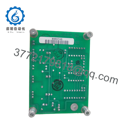
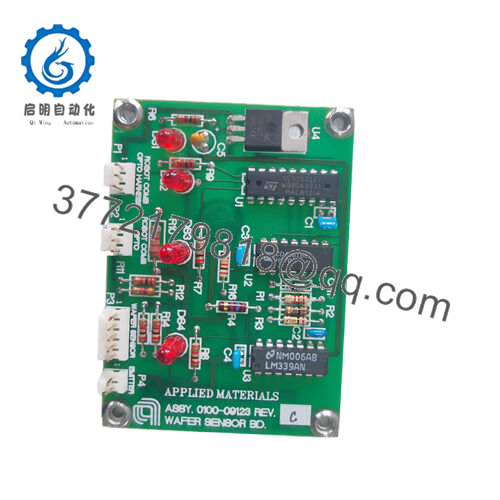
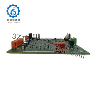
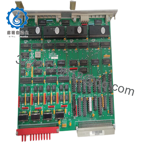
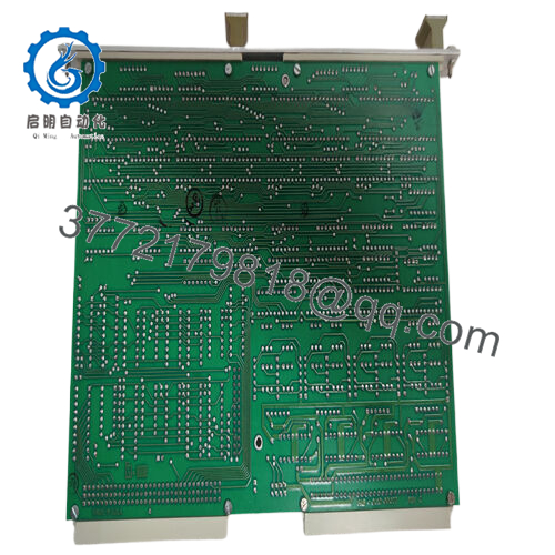
The 0100-09123 is a wafer sensor printed circuit board designed specifically for semiconductor manufacturing applications. It is part of Applied Materials’ comprehensive range of products that are integral to the semiconductor fabrication process.
Model 0100-09123
Brand Applied Materials (AMAT)
Type Wafer Sensor Printed Circuit Board
Sensor Type optical sensors for position detection, capacitive sensors for surface characteristic detection
Data Processing can process sensor data and transmit it within 1 millisecond
Power Supply 5V – 12V DC
Operating Temperature 0°C – 40°C
Mountingcan be mounted on the wafer stage using screws
Dimensions 100mm x 80mm x 10mm
Weight 0.1kg
Interfaces serial interface for communication with the control system
Certifications ISO 9001 for quality management
Environmental Rating IP20 for dust protection
The 0100-09123 is a wafer sensor printed circuit board designed specifically for semiconductor manufacturing applications. It is part of Applied Materials’ comprehensive range of products that are integral to the semiconductor fabrication process.
0100-09123
In the complex architecture of a semiconductor manufacturing system, the0100-09123 serves as a vital interface between the wafer and the control system. It is equipped with sensors that can detect various parameters related to the wafer, such as position, orientation, and surface characteristics. The board then processes this data and sends it to the main control unit, which uses the information to make decisions and control the operation of other manufacturing equipment.
For engineers and technicians working in semiconductor manufacturing, the 0100-09123 is a reliable and essential component. Its compact design allows for easy integration into existing manufacturing setups, and its high – quality construction ensures long – term performance. The board is designed to withstand the harsh environment of a semiconductor fabrication plant, including temperature variations, vibrations, and electromagnetic interference.
0100-09123
Main features and advantages:
The 0100-09123 offers exceptional functional performance. Its sensors are highly sensitive, capable of detecting even the smallest changes in the wafer’s position or orientation. This high sensitivity is crucial in semiconductor manufacturing, where precision is measured in nanometers. The board also has a fast data processing speed, enabling it to quickly analyze the sensor data and send it to the control system in real – time. This real – time data transfer allows for immediate adjustments to be made to the manufacturing process, minimizing the risk of defects.
In terms of hardware design, the 0100-09123 is built to last. It uses high – quality components that are resistant to wear and tear, ensuring long – term reliability. The board’s layout is optimized for efficient heat dissipation, which is important in a manufacturing environment where components can generate a significant amount of heat. The compact size of the board also makes it easy to install in tight spaces within the manufacturing equipment.
Compatibility is one of the board’s strong suits. It is designed to work seamlessly with other components in the semiconductor manufacturing ecosystem. It can interface with a variety of sensors, actuators, and control units, allowing for a high degree of flexibility in system design. The 0100-09123 also supports standard communication protocols, making it easy to integrate into existing manufacturing lines.
Long – term reliability is a key feature of the 0100-09123. The board undergoes rigorous testing before it is released, ensuring that it meets the high standards of the semiconductor manufacturing industry. Its components are selected for their durability and stability, and the board is designed to operate consistently over long periods of time. This reliability reduces the need for frequent maintenance and replacement, saving both time and money for semiconductor manufacturers.
Technical specifications:
Model 0100-09123
Brand Applied Materials (AMAT)
Type Wafer Sensor Printed Circuit Board
Sensor Type optical sensors for position detection, capacitive sensors for surface characteristic detection
Data Processing can process sensor data and transmit it within 1 millisecond
Power Supply 5V – 12V DC
Operating Temperature 0°C – 40°C
Mountingcan be mounted on the wafer stage using screws
Dimensions 100mm x 80mm x 10mm
Weight 0.1kg
Interfaces serial interface for communication with the control system
Certifications ISO 9001 for quality management
Environmental Rating IP20 for dust protection
Contact Us Phone:+86 16626708626 WeChat/WhatsApp:+86 16626708626 Email: 3772179818@qq.com
Related products:
0100 – 00003 VME Stepper Controller – Can work in tandem with the 0100 – 09123 in a semiconductor manufacturing setup. The stepper controller can be used to precisely position the wafer stage, while the 0100 – 09123 monitors the wafer’s position and orientation. The two components can communicate with each other to ensure that the wafer is always in the correct position for processing. 0100 – 11002 Digital I/O PCB Assembly – This digital input/output board can be integrated with the 0100 – 09123 to expand the control capabilities. It can be used to receive digital signals from the wafer sensor PCB and send control signals to other components in the manufacturing system, such as valves or motors. 0100 – 01098 PCBA Laser Driver II – In semiconductor manufacturing processes that involve laser – based operations, the 0100 – 09123 can work with the 0100 – 01098 laser driver. The wafer sensor PCB can detect the position of the wafer, and the laser driver can be adjusted based on this information to ensure that the laser beam is focused accurately on the wafer. 0100 – 20097 Water Leak Detector PCB Assy – In a semiconductor manufacturing environment where water – cooled equipment is used, the 0100 – 20097 water leak detector can be connected to the system along with the 0100 – 09123. If a water leak is detected, the water leak detector can send a signal to the control system, which can then take appropriate action, such as stopping the operation of the affected equipment to prevent damage to the wafer and other components. 0100 – 09003 Video Board – For applications where visual monitoring of the wafer is required, the 0100 – 09003 video board can be integrated with the 0100 – 09123. The video board can display real – time images of the wafer, allowing operators to monitor the wafer’s condition and any potential issues detected by the wafer sensor PCB.
Application areas:
In the high – stakes domain of semiconductor manufacturing, the 0100-09123 wafer sensor PCB by Applied Materials (AMAT) is a linchpin for ensuring the precision and quality of the production process. Semiconductor fabrication plants are intricate ecosystems where the smallest deviation can lead to defective chips, translating into significant financial losses.
During the lithography step, which is akin to creating the blueprint of the semiconductor device on the wafer, the 0100-09123 plays a crucial role. It accurately detects the position and orientation of the silicon wafer. Lithography tools use highly focused light sources to transfer circuit patterns onto the wafer. If the wafer is not correctly positioned, the patterns will be misaligned, rendering the chip useless. The wafer sensor PCB continuously monitors the wafer’s position, sending real – time data to the control system. This allows the lithography equipment to make minute adjustments, ensuring that the patterns are printed with nanometer – level accuracy.
In chemical – mechanical planarization (CMP), another critical process in semiconductor manufacturing, the 0100-09123 is also indispensable. CMP is used to create ultra – smooth surfaces on the wafer. The sensor PCB monitors the thickness and flatness of the wafer during the polishing process. By detecting any irregularities in the wafer’s surface, it enables the CMP equipment to adjust the pressure and rotation speed of the polishing pad. This ensures that the wafer is polished evenly, which is essential for 后续的 etching and deposition processes. A non – uniform surface can cause variations in the thickness of the deposited films or uneven etching, leading to defective semiconductor devices.
Research institutions engaged in semiconductor research also rely on the 0100-09123. When developing new semiconductor materials or exploring innovative manufacturing techniques, precise wafer handling and monitoring are essential. The wafer sensor PCB helps researchers accurately position and monitor wafers during experiments, facilitating the development of new materials with improved electrical and optical properties.
Installation and maintenance:
Before installing the 0100-09123, it is crucial to ensure that the installation area is clean and free of dust. Even a single dust particle can interfere with the sensors on the board, leading to inaccurate readings. Use anti – static precautions, such as wearing an anti – static wrist strap, when handling the board to prevent electrostatic discharge, which can damage the sensitive components. Check the power supply to ensure that it is stable and within the specified voltage range. Mount the board securely in the designated location, following the installation instructions provided.
For maintenance, regular visual inspections are recommended. Check for any signs of physical damage, such as cracks on the board or loose connections. Monitor the performance of the sensors by running periodic calibration tests. If the sensor readings deviate from the expected values, recalibrate the sensors or replace the board if necessary. Keep the board clean by using a clean, dry cloth to remove any dust or debris. Update the firmware of the board when new versions are available, but always test the new firmware in a non – production environment first to avoid any compatibility issues.

 WhatsApp: +86 16626708626
 Email: 3772179818@qq.com
 Phone: +86 16626708626